Optical Multi-Mesh Hypercube Interconnection Network
Project Motivation
As both silicon and GaAs based technologies drive device speed into the gigahertz (Ghz) frequency range, and rise times down to small fractions of nanoseconds, communications, not device speed, between subsystems and chips at higher and higher data rates are the limiting and decisive factor for performance and cost of high-speed computing systems. These limitations are manifested in both high-speed uniprocessors, as well as multiprocessing systems. For uniprocessors, higher performance is obtained from faster clock speeds. However, for systems operating in the Ghz range, electrical connections have to be treated as high frequency transmission systems. Skin effect, crosstalk, interference, and dielectric imperfections cause severe pulse distortions and attenuation, clock skew and random propagation delays. For multiprocessor design, the technological limitations of electronic interconnections are resulting in very limited communication bandwidth, low interconnect density, high power requirements, and long network latencies.
Optical interconnects offer the potential of alleviating many of the obstacles mentioned above. This research project explores the application of free-space optics to high-density chip-to-chip and board level interconnects. These levels of interconnects are requiring high bandwidth, high data rates, high interconnect density, and low error-rates far beyond the capabilities of current metallic-based interconnects and backplanes. The approach being carried out consists of (1) developing suitable optical network topologies that will take full advantage of the parallelism of free-space optics, (2) identifying efficient optical implementation techniques and required devices for their physical implementation, (3) identifying interface components, (4) developing modeling and simulation techniques that will provide a precise performance evaluation of optical interconnects, and (5) physically implementing some of the resulting networks and measuring their performance.
Project Description
In the recent past, it has become very clear that significant improvements in computer performance in the future can only be achieved through exploitation of parallel processing at all machine design levels. This includes both architectural and software innovations. On the architectural side, the reliable and efficient operation of such parallel machines require a number of problems to be solved, the most important and decisive one of them being the issue of communication. Any parallel system that applies several processors to a job must support efficient communication among the cooperating processors, and between processors and memory units, otherwise the very advantage of parallel processing would be offset by the communication bottleneck. Unfortunately, conventional electronic technology seems to be reaching its fundamental physical limits and is, therefore, unable to provide adequate communication bandwidth and degree of connectivity required for parallel processing. Even for uniprocessors, electronic technology is facing a fundamental obstacle: speed limitation of metal connections. This obstacle poses fundamental limitations on clock speed. It has been estimated that 250 MHz clock speeds are very hard to attain, and 1 GHz may be the ultimate limit for metal connections. The problem becomes even worse when powerful microprocessors enter the scene. For example, the bandwidth required for parallel communication of the latest Intel i860, a 64-bit 40 MHz CMOS microprocessor, is 2.56 GHz. No cost effective electronic technology can provide the space-bandwidth product required for parallel data transfer between such processors.
Optics, due to its three-dimensional nature and its high bandwidth possesses the potential for a permanent solution to the communication problem in parallel and distributed computing. Recent studies suggest that bandwidths, short latencies, and message throughputs may far exceed those possible with electronics. The advantages of using optical technology for communication are numerous: Since optical systems are potentially capable of transferring data at several orders of magnitude as compared to electronic systems, it is possible to multiplex data from thousands of processors over a single optical channel without causing a speed bottleneck. The multi-dimensional nature of optical systems, combined with their bandwidths, offers the possibility of building compact switching systems to interconnect a large number of channels not attainable by current technology. In addition, the unique attributes of optics, e.g., linear superposition, inherent multidimensionality, speed, short pulsewidth, bandwidth, relative immunity from electromagnetic interference, etc., present additional ``degrees of freedom" available for the design of efficient high-speed and fault-tolerant interconnection networks for parallel systems. These attributes have resulted in a major research impetus to investigate optical interconnection networks for parallel processing systems. Research in the design of optical interconnection networks using both free-space and guided wave has seen considerable growth in recent years.
Although several optical interconnection networks and techniques have been proposed and some of them demonstrated, few of them exploit optics advantages. The design issues involved with optical interconnects are quite different from the electronic ones. In particular, optics is inherently two-dimensional and an optical interconnect architecture which is designed to connect one-dimensional arrays of communicating nodes (these nodes could be processing elements (PEs) or processors and memory units), can evidently fail to exploit fully the parallelism available. Optical interconnections networks should be designed around two-dimensional input and two-dimensional output arrays so that (1) they better utilize the full space-bandwidth product of optical imaging systems, (2) they take full advantage of the parallelism of free-space optics, (3) they (3) open up new possibilities for designing faster parallel computing algorithms, and (4) they would be readily suited for the recent advances in compact, two-dimensional optical logic and opto-electronic device technologies. Recently, there has been a growing interest in optical interconnection architectures for nodes arranged in planner fashion. However, major limitations still exist. A major problem with planner network architectures is that their optical implementations require the use of both space-variant and space-invariant optical elements. Usually, the connection patterns depend on the location of the nodes in the plane. This requirement puts severe limitations on the choice of the optical components and implementations used, and consequently, a large body of existing optical networks do not fully exploit optics advantages.
In OCPPL, we are investigating the application of optical components and optical interconnection architectures to communications problems in parallel processing systems. This work covers network architectures, optical implementations, and applications. Our aim is to introduce three-dimensional optical network architectures that not only require simple optical implementations with existing optical hardware, but also satisfy the conditions stated above. There are five primary tasks for this research:
1) The mapping of space-variant one-dimensional and two-dimensional interconnection networks to space-invariant or semi-invariant three-dimensional networks that are highly amenable to optical implementations.
2) The development of cost-effective and efficient optical implementation techniques for the newly developed networks. This is followed by experimental realization of these optical network architectures in order to assess their actual feasibility and their validity.
3) The detailed evaluation of the resulting optical interconnection architectures. This includes a detailed simulation of the proposed networks architectures and their optical implementations as well as thorough performance evaluation of the physical realizations.
4) The study of novel routing algorithms and communication protocols for the 3-D optical networks
5) The study of the range of applications suitable for multi-dimensional optical networks.
Publications
A. Louri, B. Weech and C. Neocleous, “A spanning multichannel linked hypercube: a gradually scalable optical interconnection network for massively parallel computing,” in IEEE Transactions on Parallel and Distributed Systems, vol. 9, no. 5, pp. 497-512, May 1998.
A. Louri and C. Neocleous, “Incrementally scalable optical interconnection network with a constant degree and constant diameter for parallel computing,” in Applied Optics, vol. 36, no. 26, pp. 6594-6604, Sept. 1997.
A. Louri and C. Neocleous, “A spanning bus connected hypercube: a new scalable optical interconnection network for multiprocessors and massively parallel systems,” in Journal of Lightwave Technology, vol. 15, no. 7, pp. 1241-1253, July 1997.
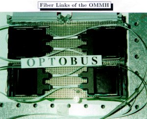
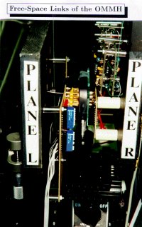
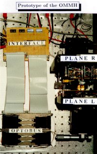
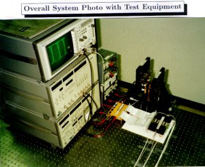
A. Louri, S. Furlonge and C. Neocleous, “Experimental demonstration of the optical multi-mesh hypercube: scaleable interconnection network for multiprocessors and multicomputers,” in Applied Optics, vol. 35, no. 35, pp. 6909-6919, Dec. 1996.