Performance-Adaptive and Power-Aware Hybrid Opto-Electronic Interconnects for HPCs
[A] Architecture and Algorithms
As communication distances and bit rates increase, opto-electronic interconnects are being deployed for designing highbandwidth low-latency interconnection networks for high performance computing (HPC) systems. While bandwidth scaling with efficient multiplexing techniques (wavelengths, time and space) are available, static assignment of wavelengths can be detrimental to network performance for non-uniform (adversial) workloads. Dynamic bandwidth re-allocation based on actual traffic pattern can lead to improved network performance by utilizing idle resources. While dynamic bandwidth re-allocation (DBR) techniques can alleviate interconnection bottlenecks, power consumption also increases considerably. In this research, we propose to improve the performance of optical interconnects using DBR techniques and simultaneously optimize the power consumption using Dynamic Power Management (DPM) techniques. DBR re-allocates idle channels to busy channels (wavelengths) for improving throughput and DPM regulates the bit rates and supply voltages for the individual channels. Taken together, this work evaluates the power-performance trade-off by balancing power consumption with improving network performance. This enables reducing communication bottlenecks, while optimizing resource utilization leading to balanced-improved system architecture design.
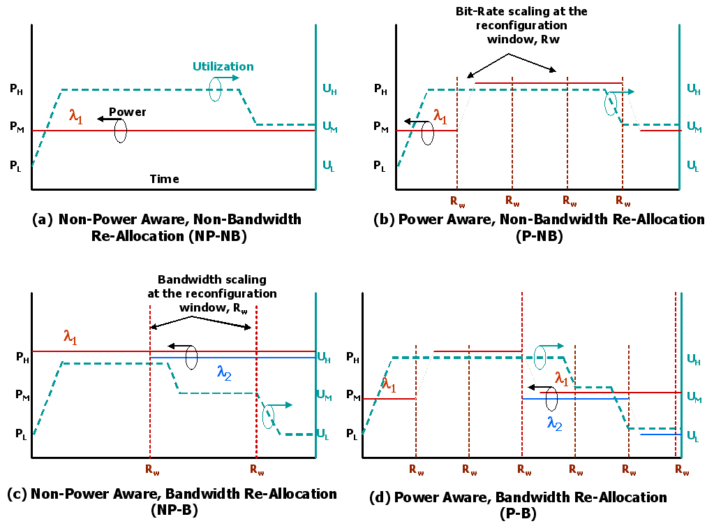
To provide more insight into power and performance trade-offs, consider Figure 1 which shows various combination of power regulation and bandwidth re-allocation techniques. These techniques include four cases namely, Non-Power Aware Non-Bandwidth Re-allocation (NP-NB), Power-Aware Non-Bandwidth Re-allocation (P-NB), Non-Power Aware, Bandwidth Re-allocation (NP-B) and Power Aware Bandwidth Re-allocation (P-B). Let us consider three power levels, namely, low-power PL, mid-power PM and high-power PH as shown on the left yaxis of Figure 1 and three link utilization levels, low-utilization UL, mid-utilization UM, and high-utilization UH as shown on the right y-axis of Figure 1. Link utilization measures the amount of time the link is in use. Moreover, assume that these link utilization levels are measured at every reconfiguration window, Rw. Reconfiguration statistics will be gathered from the past reconfiguration window to predict the future link utilization, and the corresponding power and bandwidth levels. Figure 1(a) shows the NP-NB technique. In this case, irrespective of the link utilization, the power consumption remains constant and the network cannot react to fluctuations in traffic patterns. Figure 1(b) shows P-NB technique, where the link utilization is measured at every Rw. P-NB technique allows link power to scale with link utilization. This technique is shown to reduce power consumption, but is not able to respond to increases in bandwidth demands. Figure 1(c) shows the NP-B, where the link utilization is measured at every Rw. NP-B technique allows bandwidth re-allocation to adapt to link utilization. This technique is also shown to improve performance, but is unable to regulate power. Figure 1(d) shows P-B where both power is regulated and bandwidth is re-allocated upon changes in link utilization. This technique is shown to not only reduce power, but also improve performance.
Figure - 1 : Power-regulation and Bandwidth Re-allocation Techniques
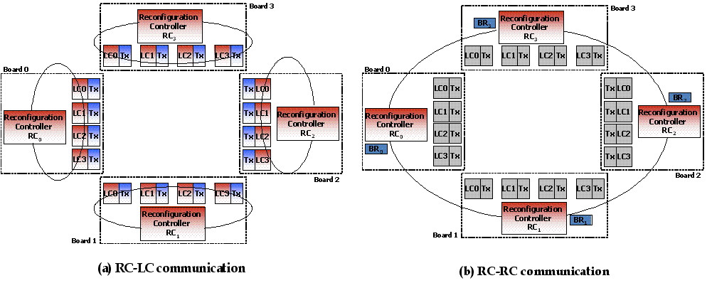
LS technique re-allocates link bandwidth, scales the bit rates and supply voltages based on historical information. In LS, each reconfiguration phase works in several circular stages, each stage is implemented either as a request or a response stage between reconfiguration controller (RC) and link controller (LC) as shown in Figure 2. Each RC triggers the reconfiguration phase, communicates with the local LCs and other RCs to determine the network load based on state information (link and buffer utilizations) collected during the previous phase. LS protocol works in the background and does not affect the on-going communication, thereby minimizing the impact of reconfiguration latency on the overall network latency.
Figure - 2 : Reconfiguration Controller (RC) and Link Controller (LC) communication
[B] Switching Techniques
In this research project we propose to investigate and design low-power, high-speed, compact non-blocking optical switches using SOI based micro-ring resonators. The row-column switch design uses row switches to exit and column switches to re-direct light to other output ports. An n´n switch requires n row switches and n column switches. Figure 3 shows a block diagram of the proposed row-column switch. As the picture depicts, the row and column switches are themselves 2 x 2 switches.
Figure 3 - n x n row-column switch
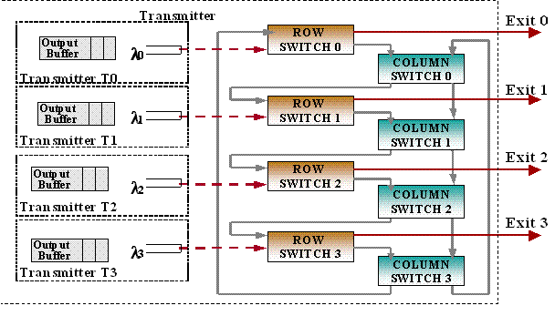
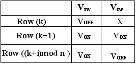
Figure 2 shows row switch k and column switch k in greater detail. A row switch requires only one ring resonator, which is resonant with the light from the corresponding transmitter (IR1). Input from the previous column switch (IR0) exits the matrix by default at (OR0). The two exit points of the row switch, (OR0) results in an outlet to leave the switch matrix, whereas (OR1) sends the signal to the corresponding column switch. Of the two inputs to the column switch IC1 is the same as OR1, while IC0 is the input from the previous column switch. There are n rings in the column switch, which enable any input signal to be routed to any one of the two outputs independent of the other signals. Of the two output signals OC1 connects to IR0 of the next row switch where as OC0 connects to IC0 of the next column switch. By suitably controlling the applied voltages, Vrw (row voltage corresponding to wavelength w), and Vc0, Vc1,..., Vcw, Vcw+1, ... , VcN-1 (column voltages corresponding to the entire wavelength set, L= l0, l1,...,lN-1) to either VON or VOFF , we can perform any-to-any switching (one-to-one, many-to-one, all-to-one) of all the wavelengths. In the row switch Vrw = VON the wavelength does not exit from OR0 of row switch k, but instead is routed to OR1. Light from OR1 is always directed towards the corresponding column switch, in this case column switch k. In the column switch, if Vcy = VON for a particular wavelength, the light does not couple to the ring resonator. As a result it goes to OC1, which will result in it exiting the switch matrix from output k+1. On the other hand if Vcw = VOFF, the light will go to OC0 and hence will proceed to the next column switch.
Figure 2 - Detailed implementation of row-column switch. IR0 (=OC0) is the input from the previous column switch, IR1 is input from transmitter, OR0 is the exit point from the switch matrix, OR1 is the input to next column switch, OC1 leads to the next column switch. Vrw and Vcw correspond to row and column voltages respectively for wavelength w. The solid line proceeds to the next column switch while the dotted line proceeds to the next row switch.
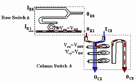
Table 1: Truth table for row and column voltages for switching between multiple outputs. VOFF is switch voltage for resonant coupling, VON is switch voltage to prevent coupling and x stands for don’t care
[C] Implementation Results
The worst case traffic pattern for E-RAPID is complement traffic, where all nodes on a given source board communicate with a destination board. For a 64 node network, nodes 0, 1, 2 ... 7 on board 0 communicates with node 63, 62, 61, ... 56 on board 7. Therefore, the network is saturated even for low load for E-RAPID architecture. As seen, NP-NB and P-NB, the network is saturated at very low loads. The throughput remains the same for both NP-NB and P-NB. With reconfiguration, all the remaining links can be provided to the system board, i.e. NP-B and P-B provide improved performance in terms of throughput. We achieve almost 400% improvement in throughput by completely reconfiguring the network. For complement traffic, P-B and NP-B techniques show superior saturation values of 0.5 as opposed to P-NB and NP-NB, where the network is saturated for extremely low load of 0.1. For complement traffic pattern, the power dissipated improves from 50% for low network loads to 20% at high loads. At high loads, bandwidth re-allocation causes more links to be active, thereby consumes more power. In E-RAPID architecture, power regulation and bandwidth re-allocation allows the network, not only to improve performance by re-allocating idle links, but also to save power by bit rate and voltage scaling. NP-B allows simply the bandwidth to be re-allocated, and P-NB allows only power to be scaled. This new P-B allows both, power as well as bandwidth to be reconfigured leading to improved network performance.
Publications
A. Kodi and A. Louri, “Performance adaptive power-aware reconfigurable optical interconnects for high-performance computing (HPC) systems,” Supercomputing, 2007. SC ‘07. Proceedings of the 2007 ACM/IEEE Conference on, Reno, NV, 2007, pp. 1-12.
C. Kochar, A. Kodi and A. Louri, “Proposed Low-Power High-Speed Microring Resonator-Based Switching Technique for Dynamically Reconfigurable Optical Interconnects,” in IEEE Photonics Technology Letters, vol. 19, no. 17, pp. 1304-1306, Sept. 2007.
C. Kochar, A. Kodi and A. Louri, “Implementation of Dynamic Bandwidth Re-allocation in Optical Interconnects using Microring Resonators,” in Proceedings of the 15th Annual IEEE Symposium on High-Performance Interconnects (HOTI 2007), Stanford, CA, 2007, pp. 54-64.
A. K. Kodi and A. Louri, “Power-Aware Bandwidth-Reconfigurable Optical Interconnects for High-Performance Computing (HPC) Systems,” in Proceedings of the 2007 IEEE International Parallel and Distributed Processing Symposium, Long Beach, CA, 2007, pp. 1-10.
A. K. Kodi and A. Louri, “