Emerging Interconnects Technologies for Network-on-Chips
Current Researchers: TBD;
There is a shift from multi-core to many-core architectures containing hundreds to a thousand cores on a single chip. However, traditional on-chip metallic interconnects require excessive power as technology keeps scaling and will not be able to provide communication support for manycore architectures.
Moreover, fundamental signaling limitations (reflections, crosstalk), electromagnetic interference (EMI), clock skew, and other problems associated with metallic interconnects will only exacerbate the power dissipation problem and thereby limit the performance of future manycore processors.
Emerging interconnect technologies such as silicon-photonics and wireless interconnects are under serious consideration for meeting the manycore communication requirements. However, the use of a single interconnect technology is not sufficient to provide satisfactory performance. Silicon photonic on-chip interconnects offer low latency, low power consumption, and high bandwidth for on-chip communication. But, they suffer from scalability difficulties and high optical power loss (insertion loss) when scaled to thousands of cores. On the other hand, on-chip wireless interconnects have the advantages of distance-independent energy consumption. But, limited frequency spectrum and higher energy/bit limit the use of wireless technology.
In this project we are leveraging the advantages of both wireless and photonic technologies, and exploring a network-on- chip called OWN (Optical Wireless Network) architecture for many-core systems. We are designing silicon photonic links for communication among the neighboring cores in a cluster of tiles with relatively short distances, and reconfigurable wireless links for inter-cluster while for inter-cluster communications and long distances on the chip.
J. Wu, A. K. Kodi, S. Kaya, A. Louri and H. Xin, “Monopoles Loaded With 3-D-Printed Dielectrics for Future Wireless Intrachip Communications,” in IEEE Transactions on Antennas and Propagation, vol. 65, no. 12, pp. 6838-6846, Dec. 2017.
We propose a novel antenna design enabled by 3-D printing technology for future wireless intrachip interconnects aiming at applications of multicore architectures and system-on- chips. In our proposed design we use vertical quarter-wavelength monopoles at 160 GHz on a ground plane to avoid low antenna radiation efficiency caused by the silicon substrate. The monopoles are surrounded by a specially designed dielectric property distribution. This additional degree of freedom in design enabled by 3-D printing technology is used to tailor the electromagnetic wave propagation.
As a result, the desired wireless link gain is enhanced and the undesired spatial crosstalk is reduced. Simulation results show that the proposed dielectric loading approach improves the desired link gain by 8- 15 dB and reduces the crosstalk by 9-23 dB from 155 to 165 GHz. As a proof-of- concept, a 60 GHz prototype is designed, fabricated, and characterized. Our measurement results match the simulation results and demonstrate 10-18 dB improvement of the desired link gain and 10-30 dB reduction in the crosstalk from 55 to 61 GHz. The demonstrated transmission loss of the desired link at a distance of 17 mm is only 15 dB, which is over 10 dB better than the previously reported work.
Ashif I. Sikder, Avinash K. Kodi, and Ahmed Louri. 201616. Reconfigurable Optical and Wireless (R-OWN) Network-on-Chip for High Performance Computing. In Proceedings of the 3rd ACM International Conference on Nanoscale Computing and Communication (NANOCOM ‘16). ACM, New York, NY, Article 25, 6 pages.
With the scaling of technology, the industry is experiencing a shift from multi-core to many-core architectures. However, traditional on-chip metallic interconnects may not scale to support these many-core architectures due to the increased hop count, high power dissipation, and increased latency. Recently, attention has recently been shifted to emerging technologies such as optical and wireless interconnects for future on-chip communications. Although emerging technologies show promising results for power-efficient, low-latency, and scalable on-chip interconnects, the use of single technology may not be sufficient to support future many-core architectures.
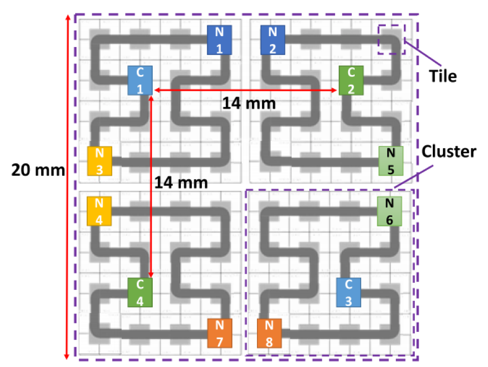
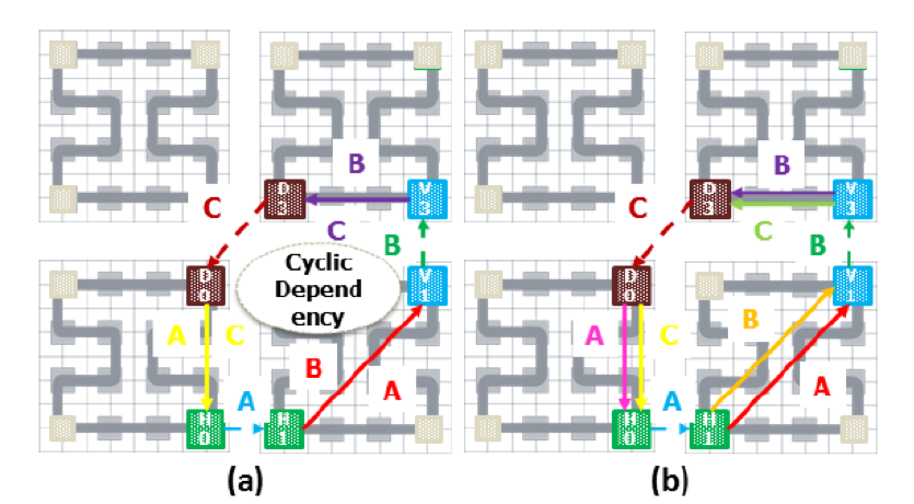
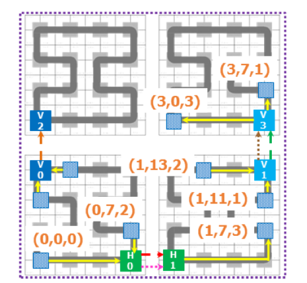
In this paper, we propose a Reconfigurable Optical-Wireless Network-on- Chip (R-OWN) that facilitates communication through static optical links and reconfigurable wireless links. The network diameter of R-OWN is restricted to three hops by dividing the network into several optical domains of 64-cores (called a cluster) and by connecting the clusters using one-hop wireless network. The optical bandwidth is efficiently shared using time division multiplexing (TDM), and the wireless bandwidth is shared using frequency division multiplexing (FDM). Packets routed across optical and wireless networks are proved to be deadlock-free. Our results indicate that R- OWN improves energy-efficiency by 44-51%, performance (throughput and latency) by 13- 31%, and area by 4-13% when compared to state-of- the-art wired, wireless, optical, and hybrid on-chip networks.
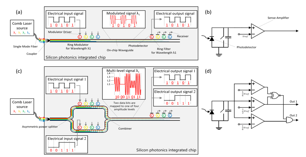
T. J. Kao and A. Louri, Optical Multilevel Signaling for High Bandwidth and Power-Efficient On-Chip Interconnects,” in IEEE Photonics Technology Letters, vol. 27, no. 19, pp. 2051-2054, Oct.
Network-on- chip (NoC) is a key component for boosting the system performance of future chip multiprocessors. With the projected increase in the number of cores on the chip, the NoC is perceived to be the limiting component for performance and scaling. Photonic NoCs are under serious consideration for scaling future multicore architectures. In this paper, we propose two photonic NoC architectures based on an optical multilevel signaling technique that can double the transmission bandwidth and reduce the area requirements. Simulation studies show that the proposed methodology saves up to 53% of power and reduces the area overhead by as much as 81% compared with metallic-based NoCs.
R. W. Morris, A. K. Kodi, A. Louri and R. D. Whaley, “Three-Dimensional Stacked Nanophotonic Network-on-Chip Architecture with Minimal Reconfiguration,” in IEEE Transactions on Computers, vol. 63, no. 1, pp. 243-255, Jan. 2014.
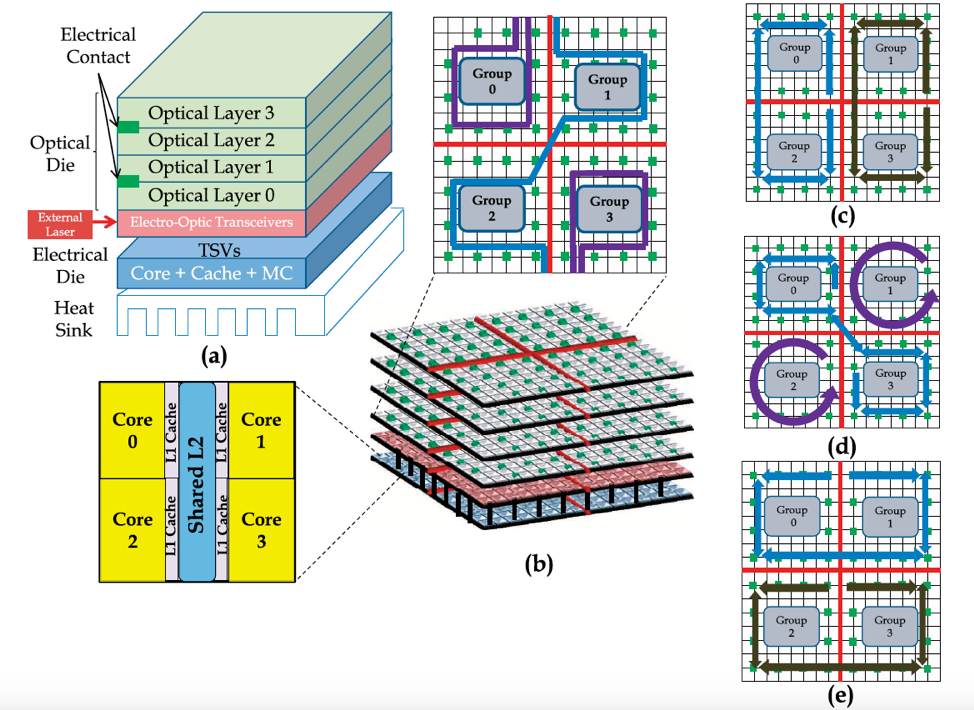
As throughput, scalability, and energy efficiency in network-on- chips (NoCs) are becoming critical, there is a growing impetus to explore emerging technologies for implementing NoCs in future multicore and many-core architectures. Two disruptive technologies on the horizon are nanophotonic interconnects (NIs) and 3D stacking. NIs can deliver high on-chip bandwidth while delivering low energy/bit, thereby providing a reasonable performance-per- watt in the future. Three-dimensional stacking can reduce the interconnect distance and increase the bandwidth density by incorporating multiple communication layers. In this paper, we propose an architecture that combines NIs and 3D stacking to design an energy-efficient and reconfigurable NoC.
We quantitatively compare the hardware complexity of the proposed topology to other nanophotonic networks in terms of hop count, network diameter, radix, and photonic parameters. To maximize performance, we also propose an efficient reconfiguration algorithm that dynamically reallocates channel bandwidth by adapting to traffic fluctuations. For 64-core reconfigured network, our simulation results indicate that the execution time can be reduced up to 25 percent for Splash-2, PARSEC, and SPEC CPU2006 benchmarks. Moreover, for a 256-core version of the proposed architecture, our simulation results indicate a throughput improvement of more than 25 percent and energy savings of 23 percent on synthetic traffic when compared to competitive on-chip electrical and optical networks.